A team of international scientists from China, Germany, Norway and Pakistan with SESAME staff have used the BM08 – XAFS/XRF beamline at SESAME for high dielectric constant materials that are of particular interest as indispensable components in electronics. The authors have demonstrated a new approach for optimizing the dielectric properties by acceptor–donor co-doping in (Gax, Cuy) Zn1−x–yO films fabricated with pulse laser deposition (PLD) or, alternatively, exchanging the co-doping step by ion implantation. Exploitation of defect engineering in dielectric ceramics for enhancing performance is an active research area globally. Materials with high dielectric constant (k) and low loss throughout a wide frequency range are among the key components for the device size scale-down in nanoelectronics. The XAFS study performed at SESAME revealed the formation of the defect dipoles around dopants.
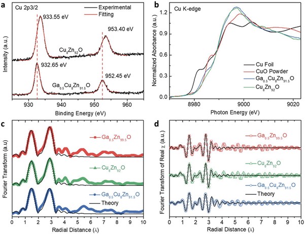
Examples of the X-ray analysis. a) XPS data showing the Cu 2p spectra for the Cu8Zn92O and Ga0.5Cu8Zn91.5O films. b) The X-ray absorption near edge structure (XANES) spectra at the Cu K-edge of Cu8Zn92O and Ga0.5Cu8Zn91.5O samples including reference samples, e.g., Cu foil and CuO powder. c) Magnitude of the Fourier transform of the extended X-ray absorption fine structure (EXAFS) spectra. d) Fourier transform of Real χ at the Zn K-edge of Ga0.5Zn99.5O, Cu8Zn92O, and Ga0.5Cu8Zn91.5O samples compared with theoretical model (black lines).
The full article may be found at https://doi.org/10.1002/smll.202107168.